
Page 2 - EMCORE-Broadband-Fiber-Optics-Brochure
P. 2
Indium Phosphide (InP) Wafer Fab
Telecom, DATA ceNTeR & liDAR cHiP DeViceS, VeRTicAlly-iNTeGRATeD mANufAcTuRiNG
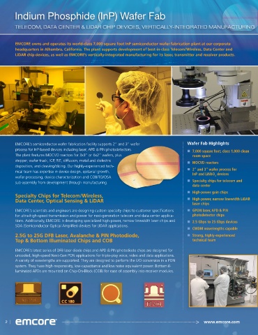
EMCORE owns and operates its world-class 7,000 square foot InP semiconductor wafer fabrication plant at our corporate
headquarters in Alhambra, California. The plant supports development of best-in-class Telecom/Wireless, Data Center and
LiDAR chip devices, as well as EMCORE’s vertically-integrated manufacturing for its laser, transmitter and receiver products.
EMCORE’s semiconductor wafer fabrication facility supports 2” and 3” wafer Wafer Fab Highlights
process for InP-based devices including laser, APD & PIN photodetectors. n 7,000 square foot, class 1,000 clean
The plant features MOCVD reactors for 3x3” or 6x2” wafers, plus room space
stepper, wafer track, ICP, RIE, diffusion, metal and dielectric n MOCVD reactors
deposition, and cleaving/dicing. Our highly-experienced tech-
nical team has expertise in device design, epitaxial growth, n 2” and 3” wafer process for
InP and LiNbO devices
wafer processing, device characterization and COB/TO/OSA 3
sub-assembly from development through manufacturing. n Specialty chips for telecom and
data center
n High-power gain chips
Specialty Chips for Telecom/Wireless,
Data Center, Optical Sensing & LiDAR n High-power, narrow linewidth LiDAR
laser chips
EMCORE’s scientists and engineers are designing custom specialty chips to customer specifications n GPON laser, APD & PIN
for ultra-high-speed transmission and power for next-generation telecom and data center applica- photodetector chips
tions. Additionally, EMCORE is developing specialized high-power, narrow linewidth laser chips and n 2.5 Gbps to 25 Gbps devices
SOA (Semiconductor Optical Amplifier) devices for LIDAR applications.
n CWDM wavelengths capable
2.5G to 25G DFB Laser, Avalanche & PIN Photodiode, n Strong, highly-experienced
Top & Bottom Illuminated Chips and COB technical team
EMCORE’s latest series of DFB laser diode chips and APD & PIN photodiode chips are designed for
uncooled, high-speed Next-Gen PON applications for triple-play voice, video and data applications.
A variety of wavelengths are supported. They are designed to perform the E/O conversion in a PON
system. They have high-responsivity, low-capacitance and low noise equivalent power. Bottom il-
luminated APDs are mounted on Chip-On-Block (COB) for ease of assembly into receiver modules.
2 | > www.emcore.com